

Here’s my schematic and board design for a simple high side switch using a P channel mosfet. It’s a simple circuit that has a input for positive and negative and an output for positive and negative connections. Pretty self explanatory. It seems like every time I go to work with mosfets I have to spend a good 5-10 minutes reminding myself how they work. So here’s a reminder to myself for the next time I go looking.
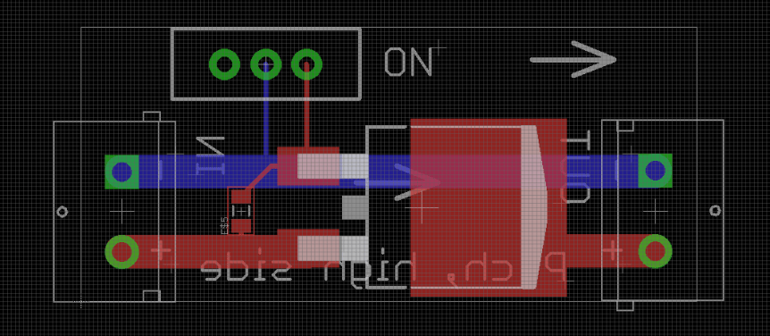
You can download the board file here. I accidentally made the pad for the mosfet as a D2PAK rather than a DPAK2. And while DPAK, DPAK2, and DPAK3 are all about the same size (almost the same size as a TO-252), the D2PAK is a much larger size. Whoops! For reference, the mosfet I’m currently using is this, where the input is 8V and using a fet with a gate to source threshold voltage of -3V and a maximum gate to source voltage of -20V. I like using a P channel mosfet for this since the circuit I care about is not connected to power. If you used a low side switch then the power would be connected and any stray connection to ground could fry everything.
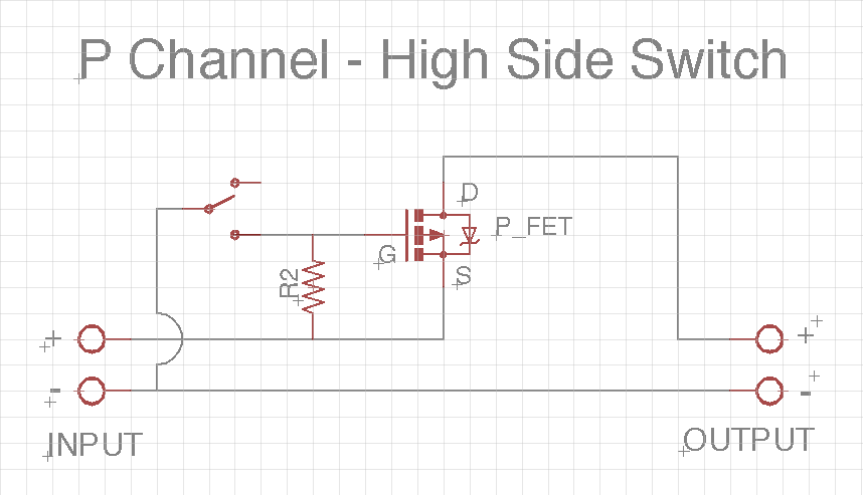
The key thing here is that the negative line passes straight through which keeps everything grounded. The switch blocks the current from flowing on the high side until the switch is flipped. R2 is a resistor that pulls the gate up to the input positive voltage (8v) so that if the switch become disconnected things don’t go crazy. When the switch is open the Vgs is zero so no current flows through the fet. When the switch is closed, the gate goes to Ground and Vgs is -8V which is below (above?) the threshold so current flows through the fet.
Here are a couple good resources for fets:
Sparkfun According to Pete Mosfets
BaldEngineer Mosfets
BaldEngineer High Side Switch
Jonathan Currie Youtube – Introduciton to Mosfets
